Hello! now About Us

Analysis of the Process Characteristics of RF Switch F2932NBGP8
5/20/2025 1:50:51 AM
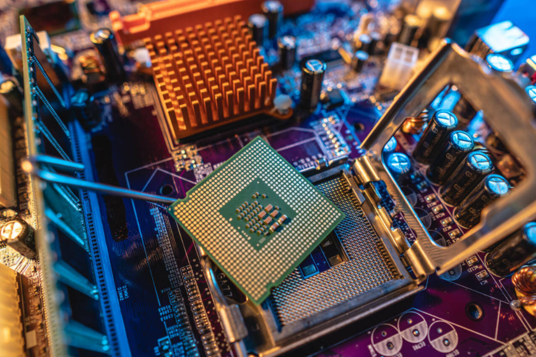
As a key component in wireless communication, satellite communication, and radar systems, the performance of RF switches directly impacts the stability and reliability of communication systems. The F2932NBGP8 RF switch, launched by Renesas Electronics' IDT division, has secured a significant position in the market thanks to its outstanding process characteristics and performance. This article will delve into the process characteristics of the F2932NBGP8 RF switch.
I. Advanced Semiconductor Manufacturing Process
The F2932NBGP8 RF switch employs an advanced semiconductor manufacturing process, ensuring its capability to operate in high-frequency bands and delivering excellent performance. Built on a silicon-based semiconductor material, the chip undergoes a complex process flow, including cleaning, stripping, oxidation, doping, diffusion, deposition, and more, to achieve precise circuit fabrication. These process steps not only enhance the chip's integration level but also optimize its electrical performance, enabling the F2932NBGP8 to operate stably across a wide frequency range from 50 MHz to 8 GHz.
II. High-Frequency Band Operation Capability
The design of the F2932NBGP8 RF switch allows it to adapt to the high-frequency bands covered by various wireless communication standards. This high-frequency band operation capability is attributed to its advanced circuit design and manufacturing process. By optimizing the circuit topology and selecting appropriate device parameters, the F2932NBGP8 achieves low insertion loss and high isolation in the on-state, thereby ensuring the quality and stability of signal transmission.
III. Low Insertion Loss and High Isolation
Insertion loss and isolation are critical indicators for evaluating the performance of RF switches. The F2932NBGP8 RF switch exhibits extremely low insertion loss for signals in the on-state, meaning that signals can maintain high energy and fidelity when passing through the switch, minimizing losses during transmission. Meanwhile, in the off-state, the F2932NBGP8 provides high isolation, effectively preventing signal leakage and mutual interference, thereby improving the signal-to-noise ratio and stability of the communication system.
IV. Fast Switching Speed
The F2932NBGP8 RF switch is capable of rapidly switching signal paths, with switching times reaching the microsecond level. This fast switching capability enables the F2932NBGP8 to promptly respond to system demands, achieving rapid signal switching and adjustment. In wireless communication systems, fast switching capabilities are crucial for supporting multi-band and multi-mode communication, ensuring that devices can flexibly switch between different network standards and maintain stable communication connections.
V. Low Power Consumption Design
With the continuous development of wireless communication devices, there is an increasing demand for low power consumption. The F2932NBGP8 RF switch adopts a low power consumption design, which helps save device energy. This low power consumption characteristic allows the F2932NBGP8 to maintain stable performance during prolonged operation while reducing the overall energy consumption of the device and extending its service life.
VI. Miniaturization and High Integration
With the continuous advancement of integrated circuit technology, the integration level of the F2932NBGP8 RF switch has become increasingly higher, and its size has become smaller. The chip adopts a 16-pin QFN package with dimensions of 4mm x 4mm x 0.9mm. Its simple rectangular shape and extremely small size make it more suitable for circuit system designs in limited spaces. This miniaturization and high integration design not only reduces system costs but also saves space, enhancing the portability and flexibility of communication devices.
VII. Wide Power Supply Voltage Range and High Reliability
The F2932NBGP8 RF switch supports a wide power supply voltage range (2.7V to 5.5V) and can operate stably across a wide temperature range from -40°C to +105°C. This wide power supply voltage range and high reliability enable the F2932NBGP8 to adapt to various harsh operating environments, ensuring the stable operation of communication systems. Additionally, the F2932NBGP8 is equipped with robust ESD protection circuits, enhancing the reliability and durability of RF systems.
The F2932NBGP8 RF switch, with its advanced semiconductor manufacturing process, high-frequency band operation capability, low insertion loss and high isolation, fast switching speed, low power consumption design, miniaturization and high integration, as well as wide power supply voltage range and high reliability, plays a vital role in wireless communication, satellite communication, and radar systems. As communication technology continues to evolve, the performance and application scope of the F2932NBGP8 RF switch will also continue to expand and improve.
Fudong Communication (Shenzhen) Group Co., Ltd., established in 2004, is a specialized global first tier semiconductor agent/distributor.
Blog Category
BlogsTags
Related Information


- 1500+ Daily average RFQ Volume

- 20,000.000 Standard Product Unit

- 1800+ Worldwide Manufacturers

- 15,000+ In-stock Warehouse
